Entegris
When it comes to handling solutions for manufacturing processes in the semiconductor and other high-technology industries, Entegris offers cutting-edge results.
The Billerica, Mass.-based company enables manufacturers to make smaller and faster microchips. The industries it serves include automotive, medical, aerospace, internet of things and electronics.
Entegris’ Advanced Materials Handling (AMH) division develops solutions to monitor, protect, transport and deliver wafers (thin slices of semiconductor material) and other substrates. It develops systems that protect wafers from abrasion, degradation and contamination during manufacturing and transportation.
“No particles. No contamination,” stresses Chris Newman, Entegris’ global 300 mm business manager. “That is the purpose of all of our products: to provide the storage and transportation from the wafer manufacturer all the way through to the finished device.”
Entegris’ two other divisions are Specialty Chemicals and Engineered Materials (SCEM) and Microcontamination Control (MC). Entegris’ AMH division produces a variety of flexible packaging and polymer containers that chemical companies use to ship process chemistries to semiconductor fabrication plants.
Its portfolio includes packaging products that include low-volume containers to transport high-value photoresist chemistries and large intermediate bulk containers for high-volume chemical consumption. Entegris solutions address automation, contamination and productivity concerns in anything from 100mm to 300mm FABs (fabrication laboratories).
“Entegris provides the tools that keep wafers clean and pristine for all the different processes,” says Sharon Harnisch, senior manager of solutions marketing, Advanced Material Handling and global marketing. “We have secret formulas in some of our products that make them cleaner and we use special materials.”
Transporting Wafers
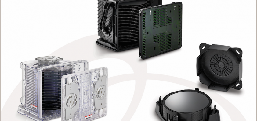
One solution for transporting wafers is the front opening unified pod (FOUP). This specialized enclosure is designed to hold silicon wafers safely and securely in a controlled environment while they are being transported and transferred into hundreds of sophisticated process steps. Within the integrated circuit semiconductor industry, device integration complexity is increasing and device structures are becoming more complex.
 As a result, contamination level requirements on substrate surfaces become more demanding. Companies can lose large sums of money due to product contamination. Molecules such as water, oxygen and other airborne molecular contaminants have become detrimental in specific process conditions.
“Ten years ago, the FOUP was being used to manage primarily particle control,” says Gary Gallagher, senior director of technology. “Today, it not only manages particle control but we’ve gone to essentially process chamber control including static protection, white light shielding and minimizing molecular contaminates. We’ve also introduced nitrogen into the FOUP to control humidity and oxygen. The devices manufacturers use are extremely sensitive to moisture and oxygen.”
Requirements for transporting silicon wafers have become more demanding, meaning fewer particles allowed per wafer. At the same time, devices have shrunk in recent years, resulting in them becoming more sensitive to particle contamination. “A nanometer size particle can kill a device,” Gallagher says. “Today it is feasible to pack 30 billion transistors on a single chip in semiconductor manufacturing. An analogy is a single particle the size of a dime in New York City that can impact device yield. “Particle control is crucial.”
A Contactless Solution
Once the product is ready to be shipped to the consumer, Entegris offers a number of back-end solutions. They include Entegris’ newest contactless horizontal wafer solution, released in 2016. An advanced solution for storage and transport of highly sensitive wafers, it provides protection against ionic, outgassing and mechanical elements and maintains wafer integrity during transport, storage or shipping.
The 300mm SmartStack Horizontal Wafer Shipper protects finished wafers in full, thin or ultrathin thicknesses and can accommodate up to 25 wafers. It is ergonomic and made from low ionic/outgassing STAT-PRO 100M material.
“The contactless horizontal wafer shipper allows our customers to ship standard, lens or bumped wafers without using Tyvek separators and PE (polyethylene) foam cushions,” says Doug Moser, manager for finished wafer products. “There are other contactless solutions on the market, but our ring design encapsulates the wafer. Our competitors’ rings are placed on top of the wafer which essentially transfers damage to the wafer in a shock event.”
The perimeter support ring minimizes the potential for surface area damage and interleaf ESD contamination to finished wafers. It also eliminates the likelihood of scuffed or marred wafers or bump damage.
Continued Investments
Entegris places heavy emphasis on research and development. The company’s continuous goal is to help its clients improve their productivity, performance and technology by providing yield-enhancing materials and solutions for the most advanced manufacturing environments.
“A one percent improvement in yield represents hundreds of millions of dollars in potential savings,” Gallagher says. “Every percentage point in yield improvement is dramatic for our customers.”
The company continues to make investments into innovative technologies, especially in 300mm wafer advancements. It partners with industry leaders in the semiconductor and other high-tech industries to take advantage of the latest advances in microcontamination control, critical materials handling and advanced process materials.
“We have R&D agreements with end-users and we work with a lot of universities and leading technology companies to improve technologies for the industry,” Newman says.