How Heraeus Electronics is advancing materials for higher-performance power electronics

With a legacy of innovative excellence spanning over three centuries, Heraeus has powered progress across several global industries. From its origins as a pharmacy in 1660 to its role today as a global, privately owned materials and technology group, Heraeus develops materials, products, and solutions that work behind the scenes within technologies that keep the world moving. From medical devices and semiconductors to smartphones, fiber-optic networks, modern vehicles, and industrial systems, the company’s expertise spans healthcare, electronics, industrial applications, and precious metal technologies, helping customers improve performance, reliability, resource efficiency, and sustainability.
Within this global portfolio, Heraeus Electronics focuses on materials for electronic packaging, an increasingly critical area as electronic devices become more powerful, compact, and demanding. By developing advanced materials and solutions for electronics and data center applications, the division helps to enable the reliable performance of the technologies powering an increasingly connected world.
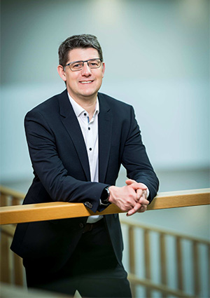
Advancing innovation at Heraeus Electronics is Dr Michael Jörger, Global Head of Technology. Having graduated as a chemist from the University of Karlsruhe and completing his PhD in material sciences, Michael spent 15 years working in Heraeus Electronics’ product development before being appointed to his current position in February 2026. Now, with data centers being an increasing focus for the company, Manufacturing Today sits down with Michael to discuss the importance of material science in AI-dependent infrastructure and how Heraeus Electronics’ ongoing developments align with market demands.
“If the forecasts for the growth of global AI usage prove accurate and we continue using AI at the current rate, we would need to install roughly 400 additional nuclear power plants. There are around 400 nuclear power plants in operation worldwide today, so this gives you an idea of the scale involved. Alternatively, we’d need to cover an area equivalent to the entire island of Mallorca with solar panels simply to generate the additional energy required,” Michael reveals. “At the moment, our focus is on increasing the efficiency of converting high voltage into low voltage as required by the chip. We’re moving towards higher voltages because it allows us to operate at lower current, reducing overall electrical losses.
“At the same time, we are trying to operate at higher temperatures and higher frequencies, while continually improving efficiency. The shift toward silicon carbide and gallium nitride semiconductors, which can operate at higher temperatures and frequencies, also requires changes to the packaging materials surrounding them. If the semiconductor operates at a higher temperature, the other materials in the package must also be capable of withstanding those temperatures. As a result, we are moving from soldering to sintering, from DCB metal-ceramic substrates to AMB metal-ceramic substrates, and from aluminum wires to copper wires. In other words, the packaging materials themselves are what enable the efficiency gains and higher operating temperatures.”
Although improving the efficiency and performance of the underlying power electronics will be essential to limiting the exponential energy footprint of AI and data centers, semiconductor advancement is only part of the solution. As Michael explains, the materials and packaging surrounding them must also evolve to support higher voltages, temperatures, and frequencies while minimizing electrical losses.
“External companies produce the chips, which then need to be integrated into power modules and converted into functional electronic devices; all the packaging materials surrounding these components, including wires, sinter paste, and solder paste, come from us. We develop and optimize these materials to make them compatible with increasingly demanding operating conditions, particularly higher temperatures,” he details. “Key considerations include matching the coefficient of thermal expansion (CTE), as well as achieving higher electrical and thermal conductivity to ensure that heat can be effectively dissipated. CTE matching is particularly important because these devices experience repeated temperature changes when they are switched on and off. The materials expand and contract, and if the CTEs do not match, there is a risk of cracking or delamination.
“At the substrate level, we also focus on thermomechanical stability, ensuring that there is no bowing, bending, or warping. Ultimately, all these material properties contribute to greater longevity and higher reliability as the performance requirements of these systems continue to increase.”
Innovation is at the core of Heraeus Electronics’ operation, as the company continues to develop materials that enable more compact designs while also reducing energy requirements. One recent example is its Welco solder paste portfolio, which enables improvements in miniaturization, reliability and sustainability.

“Our Welco solder pastes are unique materials because they use ultra-fine, highly homogeneous, spherical solder powder. These characteristics allow for smaller and more miniaturized system designs, which in turn can help save resources, and they also result in highly reliable, zero-defect packaging,” Michael says.
“We are also working on alloys that melt at lower temperatures, which can reduce energy consumption, as well as alloys that can be soldered in air rather than under nitrogen,” he reveals. “These are the kinds of projects we are pursuing to reduce operating costs and to contribute to our as well as our customer’s sustainability targets.”
As high-performance computing continues to reshape the digital landscape, it’s clear that Heraeus Electronics is providing vital solutions that enable higher power densities, temperatures, voltages, and frequencies. Through continued innovation, the company demonstrates how materials play an integral role in building a more efficient, reliable, and sustainable future for AI infrastructure and the wider electronics industry.
“I think it’s important to recognize that there is no longer any individual component operating in isolation,” Michael states. “We need to have a core development process that brings together advances in semiconductors and packaging materials, as well as packaging materials and module designs. We want to develop towards becoming a kind of solution provider, where our materials can contribute to the overall advancement of the system.”
“From the perspective of a materials supplier, I would like people to see us as a strategic enabler of system performance,” Michael concludes. “Our materials are used directly in manufacturing and assembly, and we are challenged by our customers to print faster at lower temperatures and achieve greater precision. All these challenges require close collaboration between manufacturers, equipment makers, and material suppliers. I think the right partnerships between these three groups are essential to unlocking the full potential of the technology and enabling the next generation of systems.”