
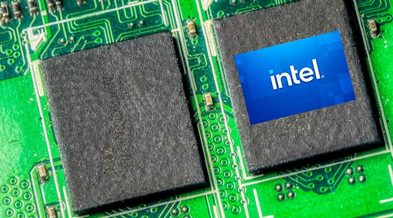
Intel Attracts Interest for Test Chips Using New Manufacturing Process
Subscribe to our free newsletter today to keep up to date with the latest manufacturing news.
Intel is drawing interest across the semiconductor industry with its upcoming 14A manufacturing process, which integrates high-numerical aperture extreme ultraviolet (high-NA EUV) lithography for the first time. Announced at Intel’s Direct Connect conference in April 2025, the development represents a strategic shift in Intel’s bid to compete directly with leading foundries.
Several customers have committed to building test chips using the 14A process. The use of high-NA EUV enables smaller, denser, and more energy-efficient transistors, allowing Intel to catch up with or surpass other advanced semiconductor manufacturers.
Intel’s 18A process advances with early production success
Parallel to 14A development, Intel’s 18A process has entered risk production, with initial wafers delivered ahead of schedule from its Arizona fabrication facility. This milestone reflects steady progress in Intel Foundry Services’ strategy to establish leadership in advanced manufacturing.
Oregon and Arizona sites are now simultaneously ramping up production capacity. 18A is expected to be the final Intel node using traditional EUV tools before high-NA EUV becomes standard in 14A. The node is also part of the US Department of Defense’s RAMP-C program, signaling trust in Intel’s readiness for secure chip manufacturing.
Intel’s foundry strategy gains traction under new leadership
Intel’s foundry resurgence is guided by CEO Pat Gelsinger and Stuart Pann, president of Intel Foundry, with support from Vice Chair Lip-Bu Tan. Tan, known for his leadership at Cadence and Walden International, brings startup-savvy insight and customer-first thinking to Intel’s model.
Intel is shifting toward a “silicon to systems” approach, aiming to serve customers through integrated chip design, manufacturing, and packaging solutions. This model allows customers to streamline production through a single partner.
Intel’s use of high-NA EUV in 14A process attracts interest
The introduction of high-NA EUV lithography in the 14A node marks one of Intel’s most aggressive technical bets. High-NA tools from ASML enable chipmakers to print smaller, more precise features, which increases transistor density and improves energy efficiency.
Intel is among the first companies to receive and install the Twinscan EXE systems required for high-NA production. Early access to this equipment is allowing Intel to begin test runs while others remain in earlier stages of procurement and integration.
Intel’s 18A process sees early adoption by major tech firms
Leading technology firms including Broadcom and Nvidia are among the early testers of the 18A process. While these test chips are not yet mass produced, they signal growing industry confidence in Intel’s design toolkits and fabrication maturity.
Intel has also improved its Process Design Kit (PDK) rollout, now delivered on a quarterly cadence. This predictable release cycle enhances coordination between Intel and its customers, who increasingly demand reliable timelines for roadmap planning.
Intel’s dual-node strategy through 14A and 18A demonstrates its long-term commitment to serving both current and emerging chip design needs. The company is also expanding advanced packaging capabilities, including Foveros Direct and EMIB, which support modular chiplet design.