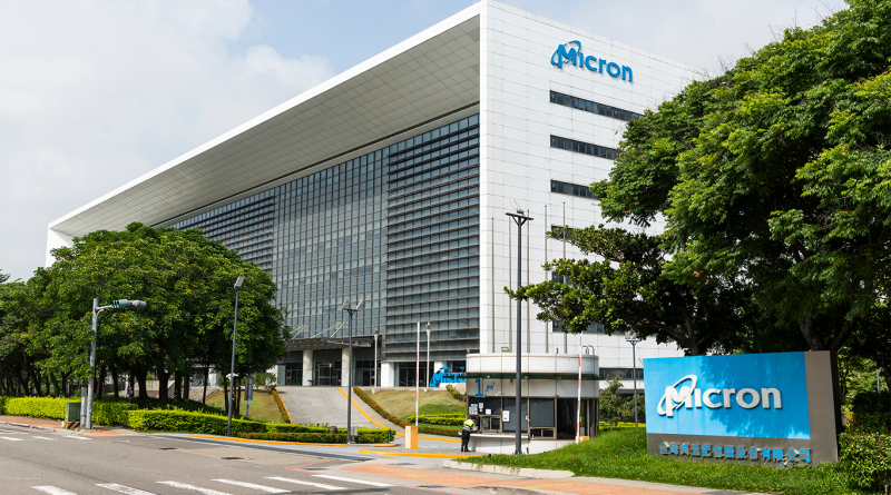
Micron to invest $10 billion in memory and semiconductor manufacturing

Subscribe to our free newsletter today to keep up to date with the latest manufacturing news.
For much of the artificial intelligence boom, the semiconductor discussion has centered on processors. GPUs, accelerators and the enormous clusters built around them have become shorthand for the computing resources required to train and run increasingly complex models.
Micron Technology is betting that the next phase of that expansion will place much greater attention on what sits beside those processors.
The company has announced Micron Research Labs, a US-based research organization headquartered in Boise, Idaho, backed by a planned $10 billion investment over the next decade. Construction of its flagship research facility is expected to begin in 2027, with space for hundreds of researchers.
The size of the commitment is significant, but the research agenda matters just as much. Micron plans to investigate memory technologies, memory and compute architectures, advanced packaging and future semiconductor manufacturing, with a research horizon extending beyond 10 years.
That scope reflects a growing challenge for AI infrastructure developers. Adding more processing capability does not automatically translate into proportional gains if data cannot reach those processors quickly enough, economically enough or within an acceptable power budget.
AI’s next hardware constraint may be memory, not compute
Modern AI systems move enormous volumes of data between processors and memory. As models grow and accelerator clusters become larger, the speed and efficiency of that movement can become a limiting factor.
Memory bandwidth determines how rapidly processors can access data. Capacity affects how much information can be kept close to compute resources. Power consumption becomes a greater concern as data centers expand. Packaging influences how physically close memory can be placed to processors and how efficiently the two can communicate.
EE News Europe identified bandwidth, capacity, power consumption and packaging as key areas coming under pressure as AI models and accelerators grow. Micron’s new laboratory is structured around many of the same technical issues.
This changes the position of memory inside the broader semiconductor market. Memory has traditionally been viewed as a component category with its own pricing cycles, production economics and product roadmaps. AI is pulling memory design closer to system architecture.
A faster accelerator is of limited use when it spends too much time waiting for data. Equally, placing greater amounts of high-performance memory close to compute resources creates its own engineering problems involving heat, energy, manufacturing complexity and cost.
That pushes semiconductor companies toward research that crosses traditional product boundaries. Micron Research Labs is intended to work across memory devices, computing architectures, packaging and manufacturing rather than treating each field as a separate problem.
The approach is visible elsewhere in Micron’s AI strategy. In June 2026, the company announced a strategic agreement with Anthropic covering memory and storage architecture design, product supply and other areas. Micron said the work directly links the requirements of frontier AI models with decisions about infrastructure design and deployment.
That relationship gives memory developers access to a clearer picture of what future AI workloads may demand. It can also give AI companies greater input into how the hardware surrounding their processors evolves.
Micron is pushing research beyond the normal product roadmap
Semiconductor companies already spend heavily on research and development, but much of that activity is tied to products and manufacturing processes expected within identifiable commercial time frames.
Micron is positioning its new research organization further upstream.
The company says Micron Research Labs will examine technologies beyond a 10-year horizon. Its Boise operation will connect with university collaborations, global satellite laboratories and research partners across government, startups and the semiconductor industry. Micron’s wider technology footprint includes operations in the US, Europe, Japan, India, Singapore and Taiwan.
That model resembles the collaborative research structures increasingly used to tackle semiconductor problems that are too expensive or technically complex for a single company to approach in isolation.
The company enters that effort with considerable intellectual property behind it. Micron says it has accumulated 62,000 patents over its lifetime. The Boise facility is expected to accommodate hundreds of researchers and host conferences, workshops and other research events.
For Micron, the attraction of long-horizon research is partly defensive. The architectures used for AI computing a decade from now may look substantially different from the systems being installed today. Memory companies that optimize only for current processor architectures risk reacting to those changes rather than helping shape them.
Advanced packaging is one area where that distinction is particularly relevant. As computing systems seek more bandwidth and lower latency, the physical relationship between processors and memory becomes more important. Packaging is no longer simply the final stage of assembling a chip. It increasingly affects system performance, energy efficiency and the economics of scaling AI hardware.
The $10 billion laboratory sits inside a much larger US investment plan
Micron’s research commitment is separate from its previously announced plan to invest more than $250 billion in US manufacturing and R&D. The company says those broader investments will support more than 90,000 jobs.
The distinction between the two programs is useful. Manufacturing investments address the ability to produce advanced memory at scale. Micron Research Labs is intended to investigate technologies that may determine what those factories need to manufacture years from now.
Together, the programs point to a semiconductor strategy that connects fundamental research, product development and domestic production.
They also come as AI infrastructure becomes a larger consideration in industrial policy. Access to processors receives much of the attention, but large-scale AI systems depend on a wider supply chain spanning memory, storage, networking, packaging, power systems and semiconductor manufacturing equipment.
Micron occupies an unusual position in that chain as the only US-based company developing and manufacturing leading-edge memory, according to the company. Its $10 billion research commitment therefore has significance beyond one new laboratory.
The more interesting question is what happens if AI development continues to pull memory research closer to processor and model design.
The Micron and Anthropic agreement already points in that direction. Instead of memory suppliers waiting for specifications to reach them through conventional product cycles, they can work with AI developers earlier in the architecture process.
If that becomes standard practice, competition in AI hardware could increasingly depend on the performance of the entire data path rather than the processor alone. The companies that determine how quickly, efficiently and economically data moves through an AI system may become just as influential as those producing the chips that perform the calculations. For Micron, $10 billion is a bet that memory will occupy a much larger part of that discussion.
Source:
EE News Europe