Newport Wafer Fab
Conducting itself the right way
With over 30 years of experience in fabricating world class, high end silicon devices under its belt, Newport Wafer Fab is a vital manufacturing service provider to a vast array of important industries and markets
Newport Wafer Fab (NWF) is the world’s first integrated silicon, and compound on silicon, wafer-fab, providing manufacturing services for the world’s first compound semiconductor cluster (CS Connected) and the wider global foundry  market. Launched in September 2017, following the successful acquisition of its present-day Newport site from Infineon Technologies, NWF is located in an impressive high technology campus in the West of Newport South Wales. The site itself has over 35 years of experience in the design, development and manufacture of semiconductor devices.
NWF is now an open-access foundry, providing volume manufacturing services for the silicon, CS and photonics markets. The largest wafer-fab in the United Kingdom, NWF can proudly call itself a start up with 36 years of RD&I, and high-volume manufacturing experience. “NWF offers foundry services to customers with compound, photonics and power semiconductor products,” confirms its Managing Director, Paul James. “We provide a foundry service to a diverse client group, ranging from large power semiconductor silicon-based customers, to bespoke photonics and compound fabless companies. The service that we provide is also varied and includes technology transfer and enhancements to process development.”
In just three years, NWF has secured contracts with ten customers and is currently ramping up silicon production processes to meet increasing demand, whilst developing technologies in power management, photonics and compound semiconductors. “What we do is offer a unique service as the world’s first foundry dedicated to compound semiconductor on silicon and silicon chip manufacturing,” Paul continues. “NWF is the device fab of the CS Connected, a collaborative and non-competitive organization located in South Wales. This compound eco-system brings together leading companies such as IQE, SPTS and Microchip, and HE institutions such as Cardiff and Swansea Universities, and the newly formed Compound Semiconductor Applications Catapult.
“This whole eco-system is also able to offer bespoke solutions utilizing compound semiconductor materials, with NWF providing the device RD&I, and scale up volume manufacturing services for the cluster. The scale and diversity of this growing Compound Semiconductor eco-system is attracting many worldwide customers who need to exploit the advantages of these new technologies.”
When it comes to the working culture of the business, NWF has benefitted from its rich history of working with a number of global organizations, while its leadership model is focused around ‘Customer First’ principles. “The Semiconductor environment demands high levels of skill and knowledge,” Paul explains. “NWF has over 400 skilled staff and has supported many through further education. This has enabled many employees to transform their lives and careers through the provision of ‘on-the-job’ development. Indeed, many of NWF’s existing managers, engineers and technicians started their careers as frontline operators. For example, we have supported over 110 staff through NVQ levels, and over 250 through Six Sigma education with local colleges. We also have an active apprentice program with six staff starting their careers in equipment engineering in 2020, and have recruited ten graduate engineers,  four at Phd Level to support our expanding RD&I portfolio. However, we believe the critical factor is our shared alues, rooted in dynamic teamwork, passion, and a collective determination to succeed.”
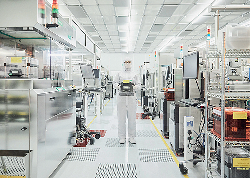
NWF is a 200mm SMIF Wafer-fab, with a current capacity of 32,000 wafer starts per month of 0.18μm and above, with an expansion capability within the existing envelope to 44,000 wafers starts per month. Its Newport site has developed a wide range of semiconductor technologies ranging from MOSFETs/TIGBTs using wafer thinning methods to CMOS, analog and compound semiconductors. NWF transfers and enhances MOSFET/TIGBT processes, and develops photonic and compound processes and devices from the initial concept/design stage through production, using systems routed in automotive methodology.
Meanwhile, with the Front-end fab, NWF benefits from a large wafer thinning and wafer test cleanroom. These additional fabs provide an integrated end-to-end service, critical to things like advanced TIGBT production. NWF adopts a range of Lean operating principles, employing many of the methods developed by Toyota, such as advanced factory automation, visual controls, constraint management, and front-line empowerment through KAIZEN and GEMBA methods.
NWF has also made a number of important infrastructure investments in recent times, not least of all its installing and commissioning of a Tri-Gen Combined Heat and Power (CHP) Plant, at a cost of approximately £3 million. “We believe that this investment alone will save the business an estimated £1 million per annum,” Paul adds. “In addition to this, NWF has installed a next generation deep trench etch system from its cluster partner SPTS. This system has been used to develop complex photonics technologies. NWF has also used its advanced equipment sets to develop GAN LEDs and GAN HEMTs technology in its 200mm fab for, and with, our compound customers and partners.”
Among the contracts signed by NWF in the last two years are a ten-year agreement with Infineon, and a seven-year contract with a second major semiconductor company. Both contracts are focused on silicon power, with many products servicing the automotive market. NWF does, however, also have intentions on broadening its portfolio of clients in other industry sectors, such as data communications and healthcare.
“With our Fabless Photonics customer partner, NWF has embarked on a project to create a novel PIC platform,” Paul details. “This development program will deliver next generation photonic transmission devices into the personal healthcare market, enabling wearable, connected technologies which promise to transform healthcare systems over the next decade.
“With our cluster partner, Cardiff University, we are also developing next generation RF MMIC (Monolithic Microwave IC’s) with leading radar and communication UK based companies. Once developed, this communications and sensor project will be scaled up at NWF in bespoke cleanrooms, with further development of RF technologies being supported via the University’s new 1500-square meter RD&I wafer-fab in Central Cardiff.”
A further item of news that it would be remiss not to mention is that NWF recently won APCUK (Advanced Propulsion Centre UK) support funding to develop low carbon technologies. Through the Automotive Transformation Fund (ATF), NWF has secured two feasibility APCUK projects to explore how NWF and its cluster partners can be scaled up to meet the UK’s ‘Net Zero 2030’ challenge. NWF, the University of Swansea and the Compound Semiconductor Centre will study the installation of a SIC (Silicon Carbide) pilot line and a major scale up to accommodate 200mm SIC and GaN on silicon for the Power/Electric Vehicle (EV) market. If supported, this will create a sovereign front-end supply chain, which is a critical need for low carbon technologies. For 14 years, the NWF site – when owned by International Rectifier – was one of the world’s leading MOSFET R&D centers, and at the heart of EV engines is a MOSFET built in a SiC substrate.
Turning his attention to the coming years, Paul highlights where he sees NWF heading. “Our ambition is to expand photonics and other compound semiconductor technologies, whilst maintaining a strong power silicon business foundation. The NWF campus offers great expansion potential within our existing building, and by re-establishing cleanrooms in the original Richard Rogers building. In addition, the 200mm wafer-fab can be further expanded to the north on ground already piled for construction. The recently awarded ‘Strength in Places’ Innovate UK award of £43 million to support the CS Cluster will also help NWF to drive the RD&I programs needed to deliver devices technologies associated with its business plan.”
In conclusion, Paul states: “Many of the applications of the Fourth Industrial Revolution will require compound semiconductors.
NWF is the device fab of the worlds’ first compound semiconductor cluster, and we believe the UK has a unique generational opportunity to deliver and lead many of the innovations that will be needed in a net zero, connected world.”
Newport Wafer Fab
Products: Wafers for silicon products