

Within its three mission pillars, AIM Photonics is shaping the future of integrated photonics in the US
As a public-private manufacturing institute, AIM Photonics focuses on the nation’s premier capabilities and expertise to capture critical global manufacturing leadership in a technology that is both essential to national security and positioned to provide a compelling return on investment to the US economy.
AIM Photonics aims to emulate successes experienced by the electronics industry over the past 40 years and transition key lessons, processes, and approaches to the Photonic Integrated Circuit (PIC) industry. By supporting small and medium enterprises, educating people, and providing practical access and technology for US industry, government, and academic communities, AIM Photonics is creating a first-of-its-kind national PIC manufacturing ecosystem. 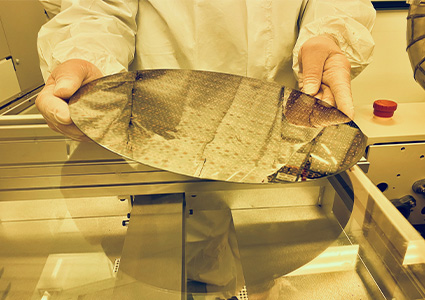
The organization is one of 18 manufacturing innovation institutes in the US, each of which is a public-private partnership supported by a combination of federal and private funding. Wade Cook, Executive Director, explains more about AIM Photonics and its purpose: “Each institute is designed to improve or enlarge the US industrial base in certain technologies or capabilities, ours being integrated photonics. As one of nine institutes funded through the Department of Defense (DoD), AIM Photonics was established in 2015 when the DoD recognized the significant need for capacity, product development, and prototyping of PICs in the US, including fabrication and packaging.
“The biggest non-federal source of funding is the State of New York, which is investing heavily in various semiconductor facilities and capabilities to bring business back to the state. We operate out of two facilities, one is an extensive research campus in Albany, which the federal government has pledged to make a center of research through the CHIPS Act. Our other facility in Rochester oversees testing, assembly, and packaging (TAP), and has benefited from a $27 million investment to add new tools and capabilities.
“We have three mission pillars: research and development (R&D), access to facilities, and education,” he states. “In terms of R&D, we’re continuously developing new and improved technologies for companies and individuals to use for product development and prototyping. Second, we have state-of-the-art facilities within our portfolio and we’re passionate about making them accessible to industry, especially to small and medium enterprises. Lastly, we have a lot of activities around educating, growing, and developing the workforce, including engineers, technicians, and advanced professionals.”
 Elaborating on the institution’s specific focus, Wade continues: “Our focus within photonics is primarily silicon photonics, which are integrated photonics made on a silicon wafer in a similar process used for electronic integrated circuits. Silicon photonics ride on the shoulders of giants in the electronic integrated circuit industry, but demand is growing rapidly for silicon photonics, which play a crucial role in data and telecom applications. With the explosive spread of AI, data centers are requiring more silicon photonics to enable faster, cooler, and lower power computing.
“There are other applications too, such as the production of small, high-sensitivity biological or chemical sensors. As part of a general trend to make medical instruments smaller and lighter, there are several blood and saliva testing apparatus currently in development to detect medical conditions at low concentrations.”
Silicon photonics are also used in quantum applications. “The focus is no longer on making larger chips, but instead producing smaller, more specialized chips, as well as multiple chiplets for quantum applications,” Wade elaborates. “The industry is predicting a mix of electronic and photonic chips, and we’re responding to this in two major ways.
“One of our main services is offering multi project wafer (MPW) schemes every quarter. An MPW works by aggregating the cost across multiple independent users, providing companies or researchers with an opportunity to purchase a number of usable chips for experimental purposes at a lower cost, as opposed to spending up to $1 million on a custom wafer.
“We’re launching two technology platforms for our MPW service in 2025. We’re implementing a major upgrade to our Base Active PIC platform, which will be useful in the near infrared wavelengths that are traditional for silicon photonics. We’re also launching our Quantum Flex (QFlex) PIC to design and produce chips specifically for quantum applications, with various features such as shorter wavelengths and the ability to transmit light.”
Talking about these new technologies leads Wade to share more details about what’s coming for AIM Photonics in the year ahead. “Aside from launching two new technology platforms for our MPW service, 2025 will also see us emphasize our HOPE kits,” he says. “We produce HOPE kits, that stands for hands-on photonics education, to be used in university laboratories and community colleges to enable students learning about photonics to test and manipulate circuits.
“Further afield, we’ll prioritize maintaining our MPW service going forward, as it is a very valuable prototyping and product development tool,” Wade concludes. “We hope to enter our third cooperative agreement once our current one ends, and we’ll continue to respond to market demand with more advanced technologies and innovative solutions.”