
Camtek
Ingenious solutions
As demand for its high-end inspection and metrology equipment increases, Camtek is looking forward to more growth in 2021
A history of innovation has made Camtek one of the technological leaders in the field of inspection and metrology for the semiconductor market. Incorporated in Israel in 1987, the company began life as a provider of optical inspection equipment to address the needs of the PCB industry before launching its first automatic inspection system for the semiconductor sector in 2003.
After building on its technologies and adding three new inspection and metrology product lines in the years that followed, Camtek sold its PCB business in 2017 and became a pure semiconductor capital equipment company. The firm is publicly traded on both the NASDAQ and Tel Aviv Stock Exchange, and offers world-class sales and customer support infrastructure across eight territories (subsidiaries).
“Technological innovation and operational flexibility have always set Camtek apart from the competition,” declares company Chairman and CEO Rafi Amit. “Our innovative solutions are tailor-made to meet our customers’ requirements and roadmaps. The fact that each solution is individually customized makes it possible to provide clients with systems that satisfy fluctuating needs, supported by short delivery time and local support worldwide.”
Camtek’s modern product range is centered around automatic inspection and metrology systems designed to detect individual dice defects on wafers before they are packaged. Sorting defected dice before packaging is a vital process for the semiconductor industry because a single device defect can cause the failure of an entire product.
Through employment of the latest technology, including advanced optics and electronics hardware, advanced algorithms and software, image processing, motion control and material handling, Camtek develops bespoke customer solutions that its competitors have yet to imagine.
Serving IDMs, OSATs and foundries in the most demanding semiconductor market segments, such as Advanced Interconnect Packaging, Memory, CMOS Image Sensors, MEMS and RF, Camtek systems inspect and measure IC and IC features on wafers throughout the semiconductor device production process.
“First, the wafers are scanned under the advanced optic heads (2D inspection and metrology and 3D metrology) in our systems,” Rafi explains. “Advanced software and algorithms are implemented on the scanned wafer’s data and then, as a result, our systems automatically sort good dies from defected dies. The defected dies are removed from the production lots and will not be inserted into a package, hence the total end product yield is enhanced by ensuring that only known good dies are shipped to end-users.
“Camtek systems are easy to operate and offer high accuracy and productivity in high volume manufacturing environments,” Rafi adds. “For extra reliability, each system is employed at various manufacturing stages starting from the front-end macro inspection and outgoing Quality Control (OQC), through inspection and metrology of bumps in the mid-end and the inspection of post-diced wafers in assembly.”
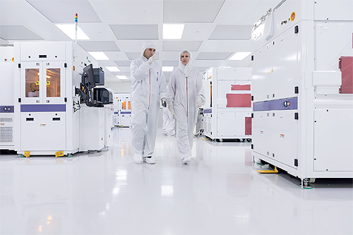
As of 2021, Camtek’s manufacturing facility is based in Northern Israel and operates in line with a two-stage production methodology. In the first stage, EMS companies build the basic parts of a machine. The second stage sees critical components assembled on the systems, before final integration is performed in clean rooms at the production facility.
In line with Camtek’s meticulous design requirements, some of the company’s optical, mechanical and electronic hardware developments are completed by its
suppliers, whereas most critical hardware components, and all detection engines and software, are developed inhouse. Before production can begin however, Camtek works closely with its key customers on the design phase of its projects.
“Our clients are developing the next generation of packaging technologies and they use our systems to make that happen,” Rafi says. “Working in collaboration with these companies allows us to understand the Advanced Packaging industry’s roadmap and design our systems and solutions accordingly. In our field, the development of new generations of products and solutions never stops. We’ve always got the next big answer in the pipeline.”
When it comes to customer support, a global, direct to customer, pre- and post-sales service is operated through subsidiaries in the US, Europe, Japan, China, Hong Kong, Taiwan, Korea and Singapore. “Our local teams are able to install our systems at customer sites, give customers ongoing support and training, as well as solve application issues,” Rafi states. “It’s a real advantage and enables us to quickly respond to our clients’ needs.
“Whether in production, sales or customer service, people are key to the company’s success,” he continues. “Our employees are extremely professional, and we always encourage creativity and out-of-the-box thinking, which leads to the development of innovative solutions.”
The bond Camtek has built with its workforce has been particularly important to both parties throughout the last 12 months. As Covid-19 threw many businesses into a state of uncertainty, Camtek and its employees across the world worked in cohesion to ensure the company’s continued prosperity.
“Things were quite unclear at the beginning of the pandemic when all countries in Asia closed their borders,” Rafi recalls. “It was not clear what was going to happen with our clients and our business back then, but I am proud to say that, thanks to the hard work and support of our local teams, we continued manufacturing and installing systems around the globe. The huge collaborative effort resulted in a record year.”
A successful 2020 capped off a period of significant growth for Camtek that has seen the business triple its revenues since 2013. Rafi believes that there are a number of key factors behind this growth, including the fact that semiconductor products have an ever-increasing presence in all areas of 21st century life.
“The semiconductor sector has become a strategic industry for the world and demand for new products is on a steady rise,” Rafi remarks. “End customers’ requirement for defect-free components has become standard, meaning manufacturers must now use inspection machines to test 100 per cent of their shipped goods.
“Our strong presence in fast-growing market segments has been greatly beneficial over the last few years and we keep increasing our market share due to technological superiority, bold leadership and the introduction of new products that address evolving customer needs and emerging applications.”
A winning combination of performance, flexibility, ease of operation and reliability means Camtek now has close to 1200 of its systems installed worldwide, serving over 100 customers, including most of the world’s major semiconductor manufacturers. In addition, the firm has an increasingly strong position in Asia, especially China, where its market segments are growing faster than anywhere else.
“Our big challenge for 2021 is to continue expanding at a rapid pace and meet the growing demand for our systems,” Rafi asserts. “We must also complete new developments that will allow us to continue to be a leading technology company and to increase our product offering through potential acquisitions.
“We expect Camtek to continue growing organically at a similar pace to recent years. In addition, we will strive to acquire companies that have synergy with Camtek, and allow us to increase product lines and expand beyond organic growth.”
Camtek Ltd
Products: Inspection and metrology equipment
www.camtek.com